NEET-XII-Physics
14: Semiconductor Electronics: Materials Devices and Simple Circuits
Note: Please signup/signin free to get personalized experience.
Note: Please signup/signin free to get personalized experience.
10 minutes can boost your percentage by 10%
Note: Please signup/signin free to get personalized experience.
- #14-aWhat will be the forward current at a forward voltage of 0.6 V?Ans : Forward voltage, V = 0.6 V
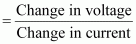
∴Current, I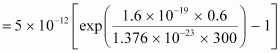
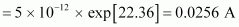
Therefore, the forward current is about 0.0256 A.
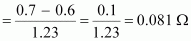
- #14-bWhat will be the increase in the current if the voltage across the diode is increased to 0.7 V?Ans : For forward voltage, V’ = 0.7 V, we can write:
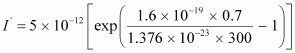
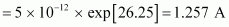
Hence, the increase in current, ΔI = I‘ - I
= 1.257 - 0.0256 = 1.23 A
- #14-cWhat is the dynamic resistance?Ans : Dynamic resistance
- #14-dWhat will be the current if reverse bias voltage changes from 1 V to 2 V?Ans : If the reverse bias voltage changes from 1 V to 2 V, then the current (I) will almost remain equal to I0 in both cases. Therefore, the dynamic resistance in the reverse bias will be infinite.
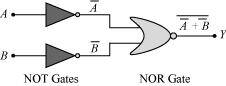
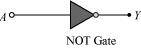
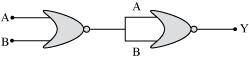
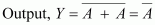
- #15-aacts asAns : A and B are the inputs and Y is the output of the given circuit. The left half of the given figure acts as the N
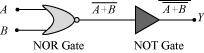
Hence, the output of the N OR Gate =
This will be the input for the NOT Gate. Its output will be = A + B
∴Y = A + B
Hence, this circuit functions as an OR Gate.
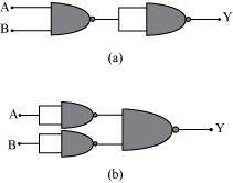
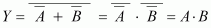
- #15-bacts as AND gate.
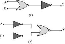
Ans : A and B are the inputs and Y is the output of the given circuit. It can be observed from the following figure that the inputs of the right half N
Hence, the output of the given circuit can be written as:
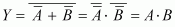
Hence, this circuit functions as an AND Gate.
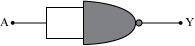
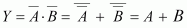
- Qstn #16Write the truth table for a NAND gate connected as given in Fig. 14.45.
Hence identify the exact logic operation carried out by this circuit.
Ans : A acts as the two inputs of the NAND gate and Y is the output, as shown in the following figure.
Hence, the output can be written as:

The truth table for equation (i) can be drawn as:
A
Y 
0
1
1
0
This circuit functions as a NOT gate. The symbol for this logic circuit is shown as:
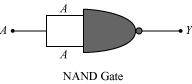
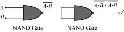
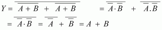
- Qstn #17You are given two circuits as shown in Fig. 14.46, which consist of NAND gates. Identify the logic operation carried out by the two circuits.
Ans : In both the given circuits, A and B are the inputs and Y is the output.
- #17-a
Ans : The output of the left NAND gate will be , as shown in the following figure.
Hence, the output of the combination of the two NAND gates is given as:
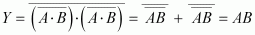
Hence, this circuit functions as an AND gate.
- #17-b
Ans : is the output of the upper left of the NAND gate and
  is the output of the lower half of the NAND gate, as shown in the following figure.
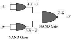
Hence, the output of the combination of the NAND gates will be given as:
Hence, this circuit functions as an OR gate.
- Qstn #18Write the truth table for circuit given in Fig. 14.47 below consisting of N OR gates and identify the logic operation
( OR , AND, NOT) which this circuit is performing.
(Hint: A = 0, B = 1 then A and B inputs of second N OR gate will be 0 and hence Y=1. Similarly work out the values of Y for other combinations of A and B. Compare with the truth table of OR , AND, NOT gates and find the correct one.)
Ans : A and B are the inputs of the given circuit. The output of the first N OR
gate is.gif) . It can be observed from the following figure that the inputs of the second N
OR
. It can be observed from the following figure that the inputs of the second N
OR
gate become the out put of the first one.

Hence, the output of the combination is given as:
The truth table for this operation is given as:
A
B
Y (=A + B)
0
0
0
0
1
1
1
0
1
1
1
1
This is the truth table of an OR
gate. Hence, this circuit functions as an OR
gate.
- Qstn #19Write the truth table for the circuits given in Fig. 14.48 consisting of N OR
gates only. Identify the logic operations ( OR , AND, NOT) performed by the two circuits.

Ans : (a) A acts as the two inputs of the N OR
gate and Y is the output, as shown in the following figure. Hence, the output of the circuit is .
.

The truth table for the same is given as:
A
Y 
0
1
1
0
This is the truth table of a NOT gate. Hence, this circuit functions as a NOT gate.
(b) A and B are the inputs and Y is the output of the given circuit. By using the result obtained in solution (a), we can infer that the outputs of the first two N OR
gates are as shown in the following figure.

 are the inputs for the last N
OR
are the inputs for the last N
OR
gate. Hence, the output for the circuit can be written as:
The truth table for the same can be written as:
A
B
Y (=A⋅B)
0
0
0
0
1
0
1
0
0
1
1
1
This is the truth table of an AND gate. Hence, this circuit functions as an AND gate.